2023-06-16 11:11:40
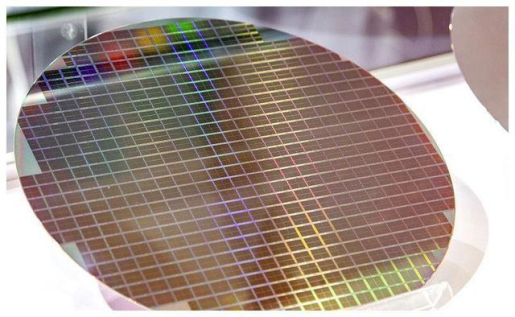
Wafer is an abbreviation for a round piece of semiconductor crystal. It is used as a carrier substrate in the integrated circuit manufacturing process, and can be processed into various circuit element structures on the wafer, and becomes an IC product with specific electrical functions.
Wafer bonding is a wafer-level packaging technology. It refers to the tight bonding of two or more homogeneous or heterogeneous wafers that have been mirror-polished through chemical and physical effects. After the wafers are bonded, the bonding The interface will achieve a specific bond strength. The package protects the sensitive internal structure of the wafer from environmental influences such as temperature, humidity, high pressure and oxidizing substances, improving the long-term stability and reliability of functional components. Wafer bonding can be used in various technical fields such as MEMS device manufacturing, microelectronics and optoelectronics, etc.
In the bonding process, there are many uncertain factors that will affect the quality of the bonding. The internal factors include the chemical adsorption state, flatness and roughness of the wafer surface, and the external factors are mainly the bonding temperature and time. The detection and characterization of bonded wafers can evaluate the technical yield, bonding strength and airtightness level. Whether it is used for manufacturing equipment or for process development, wafer bonding detection is of great significance .
The study found that short-wave infrared is very suitable for quality inspection after the wafer bonding process, and can provide users with fast and accurate non-destructive interface inspection images. Before the chip is thinned, the wafer is attached to the carrier with a temporary glue, and a bond is formed between the wafer and the carrier. Common slide materials include glass, sapphire, and silicon carbide (SiC). If there are unbonded areas (such as air bubbles) at the bonding interface between the wafer and the carrier, the incident light will be reflected multiple times on the upper and lower surfaces of the unbonded area, while the light at the normal bonding area will be directly transmitted. This difference After being processed by the camera, a clear difference between light and dark will appear on the display.
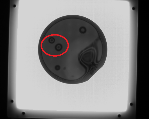
Among them, after the glass and sapphire materials are bonded to the wafer, if there are bubbles (bad bonding), they can be directly observed by human eyes or visible light cameras. When using silicon carbide slides, because the color of the material itself is translucent green, visible light cannot penetrate well and clearly observe the bubbles generated by bad bonding, but the short-wave infrared camera can at this time Works well for penetrating observations of materials. The picture below is a bonded wafer picture taken by the inspection system (model) built with the Gatherstar short-wave infrared camera:
For more information about SWIR cameras and SWIR detectors, please visit https://www.gatherstarhk.com/
Sales Manager: Lily Liu
Mobile: 086-13359283296
Email: info@gatherstarhk.com
Gatherstar Technology (HK) Ltd is specialized in infrared and laser photoelectric system products and module, components and elements. we are not only confident in supplying qualified optoelectronic products to all of our customers, but also concentrating on offering continuous innovations and reliable service.