2023-04-13 17:10:39
Short wave infrared (SWIR) cameras can detect invisible product defects and specific material characteristics, opening up a wide range of application space for machine vision solutions. Compared to mainstream machine vision cameras equipped with CMOS or CCD sensors, most SWIR cameras are equipped with InGaAs (indium gallium arsenide) sensors, with detection wavelengths ranging from 900 nm to 1700 nm. The latest sensors on the market have extended their supported spectral range to visible spectra, or exceed 1700 nm, up to 2500 nm. Light with wavelengths exceeding 750 nm belongs to the invisible spectrum of the naked eye, and traditional CCD or CMOS cameras can only detect light with wavelengths below approximately 1050 nm. Therefore, the application range of shortwave infrared cameras is wider than traditional cameras, for example, it can easily detect water accumulation inside plants or defects inside wafer products.
This article introduces the application examples of shortwave infrared cameras in multiple fields, such as the semiconductor industry, recycling, metal and glass inspection, and airborne remote sensing.
Semiconductor industry
The semiconductor industry has developed into one of the largest industries in the world, and its growth momentum has continued unabated. The production of wafer integrated circuits (ICs or chips) is the core business of the industry.
Cameras equipped with InGaAs sensors typically operate in the shortwave infrared spectral range of 900 nm to 1700 nm and can achieve spectral imaging at a wavelength of approximately 1150 nm through semiconductor materials such as silicon (Si). Therefore, shortwave infrared cameras have become essential equipment in the inspection process. Silicon wafer transparency imaging is a non-destructive testing method that provides many benefits for the production process. Nowadays, the semiconductor industry has introduced InGaAs cameras into testing, inspection, and quality control systems.
Inspection of silicon crystals and ingots
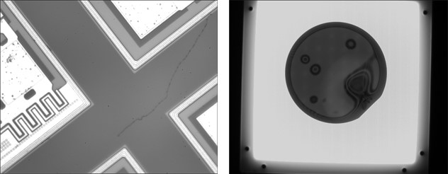
The inspection of silicon crystals and ingots (also known as crystal bricks) is one of the typical applications of InGaAs cameras in the semiconductor industry. InGaAs cameras can image the transmittance spectrum of silicon based materials (with a wavelength range greater than 1150 nm), making them an ideal solution for detecting impurities that may accumulate in crystals or crystal rods during the production process. The crystal rod needs to be cut into thin wafers using a special diamond cutting knife, and the purity of the wafer is crucial in this processing process. Even if the wafer contains only a small piece of metal or other inclusions, it can lead to the fracture and scrapping of expensive diamond cutting knives. Replacing cutting tools not only requires cost, but also leads to a decrease in production efficiency and profits. The introduction of shortwave infrared cameras can avoid this problem and ensure smooth production processes.
Wafer inspection or packaging
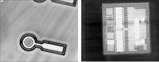
Another important application of shortwave infrared cameras is wafer inspection. In the wafer production process, particles may appear at the top, bottom, and even inside or between wafers. CCD or CMOS cameras can detect particles at the top and bottom, while InGaA cameras can detect particles between two bonded wafers through silicon based materials.
InGaAs cameras can also be used for wafer packaging, which detects whether the arrangement of the back of the wafer is aligned with the front. Short wave infrared technology can help align the layers of the wafer, as well as align the wafer substrate and other sub products, such as ICs, storage cells, or transistors.
Photovoltaic power generation
From silicon crystals to crystal rods/bricks, wafers, solar cells, and even solar modules, shortwave infrared camera applications can cover the entire supply chain inspection process. Due to its ability to achieve transparent imaging of silicon based materials, InGaAs cameras are the most effective solution for detecting internal physical defects in silicon based materials.
Recycling industry
The amount of waste generated by developed countries is constantly increasing, while the amount of available resources is becoming increasingly scarce; Therefore, it is necessary to develop effective methods to separate high-quality recyclable materials from collected waste.
Plastic sorting
Due to the roughly similar visible spectra of all plastic waste, it is not possible to separate recyclable materials using conventional methods. However, within the shortwave infrared spectrum range, the absorption spectra of different plastic materials exhibit different characteristics. Therefore, we can use shortwave infrared camera technology to build an automated separation system to separate and recover materials with similar quality and properties. The latest version of the shortwave infrared camera has expanded its spectral range to 2.5 µ m, which can distinguish more material types.
Sales Manager: Lily Liu
Mobile: 086-13359283296
Email: info@gatherstarhk.com
Gatherstar Technology (HK) Ltd is specialized in infrared and laser photoelectric system products and module, components and elements. we are not only confident in supplying qualified optoelectronic products to all of our customers, but also concentrating on offering continuous innovations and reliable service.